A
resistor is a
passive two-terminal electrical component that implements
electrical resistance
as a circuit element. Resistors act to reduce current flow, and, at the
same time, act to lower voltage levels within circuits. In electronic
circuits, resistors are used to limit current flow, to adjust signal
levels,
bias active elements, and terminate
transmission lines among other uses. High-power resistors that can dissipate many
watts of electrical power as heat may be used as part of motor controls, in power distribution systems, or as test loads for
generators.
Fixed resistors have resistances that only change slightly with
temperature, time or operating voltage. Variable resistors can be used
to adjust circuit elements (such as a volume control or a lamp dimmer),
or as sensing devices for heat, light, humidity, force, or chemical
activity.
Resistors are common elements of
electrical networks and
electronic circuits and are ubiquitous in
electronic equipment.
Practical resistors as discrete components can be composed of various
compounds and forms. Resistors are also implemented within
integrated circuits.
The electrical function of a resistor is specified by its resistance:
common commercial resistors are manufactured over a range of more than
nine
orders of magnitude. The nominal value of the resistance will fall within a
manufacturing tolerance.
Electronic symbols and notation
Two typical
schematic diagram symbols are as follows;
-
(a) resistor, (b) rheostat (variable resistor), and (c) potentiometer
-
The notation to state a resistor's value in a circuit diagram varies, too. The European notation
BS 1852 avoids using a
decimal separator, and replaces the decimal separator with the SI prefix symbol for the particular value. For example,
8k2 in a circuit diagram indicates a resistor value of 8.2 kΩ. Additional zeros imply tighter tolerance, for example
15M0.
When the value can be expressed without the need for an SI prefix, an
'R' is used instead of the decimal separator. For example,
1R2 indicates 1.2 Ω, and
18R
indicates 18 Ω. The use of a SI prefix symbol or the letter 'R'
circumvents the problem that decimal separators tend to 'disappear' when
photocopying a printed circuit diagram.
Theory of operation
The
hydraulic analogy
compares electric current flowing through circuits to water flowing
through pipes. When a pipe (left) is filled with hair (right), it takes a
larger pressure to achieve the same flow of water. Pushing electric
current through a large resistance is like pushing water through a pipe
clogged with hair: It requires a larger push (
voltage drop) to drive the same flow (
electric current).
[1]
Ohm's law
The behavior of an ideal resistor is dictated by the relationship specified by
Ohm's law:

Ohm's law states that the voltage (V) across a resistor is
proportional to the current (I), where the constant of proportionality
is the resistance (R). For example, if a 300
ohm resistor is attached across the terminals of a 12 volt battery, then a current of 12 / 300 = 0.04
amperes flows through that resistor.
Practical resistors also have some
inductance and
capacitance which will also affect the relation between voltage and current in
alternating current circuits.
The
ohm (symbol:
Ω) is the
SI unit of
electrical resistance, named after
Georg Simon Ohm. An ohm is equivalent to a
volt per
ampere. Since resistors are specified and manufactured over a very large range of values, the derived units of milliohm (1 mΩ = 10
−3 Ω), kilohm (1 kΩ = 10
3 Ω), and megohm (1 MΩ = 10
6 Ω) are also in common usage.
Series and parallel resistors
The total resistance of resistors connected in series is the sum of their individual resistance values.


The total
resistance of resistors connected in parallel is the reciprocal of the
sum of the reciprocals of the individual resistors.


So, for example, a 10 ohm resistor connected in parallel with a 5 ohm
resistor and a 15 ohm resistor will produce the inverse of
1/10+1/5+1/15 ohms of resistance, or 1/(.1+.2+.067)=2.725 ohms.
A resistor network that is a combination of parallel and series
connections can be broken up into smaller parts that are either one or
the other. Some complex networks of resistors cannot be resolved in this
manner, requiring more sophisticated circuit analysis. Generally, the
Y-Δ transform, or
matrix methods can be used to solve such problems.
[2][3][4]
Power dissipation
At any instant of time, the power
P (watts) consumed by a resistor of resistance
R (ohms) is calculated as:
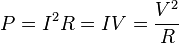
where
V (volts) is the voltage across the resistor and
I (amps) is the
current flowing through it. Using
Ohm's law,
the two other forms can be derived. This power is converted into heat
which must be dissipated by the resistor's package before its
temperature rises excessively.
Resistors are rated according to their maximum power dissipation.
Most discrete resistors in solid-state electronic systems absorb much
less than a watt of electrical power and require no attention to their
power rating. Such resistors in their discrete form, including most of
the packages detailed below, are typically rated as 1/10, 1/8, or 1/4
watt.
An aluminium-housed power resistor rated for 50 W when heat-sinked
Resistors required to dissipate substantial amounts of power,
particularly used in power supplies, power conversion circuits, and
power amplifiers, are generally referred to as
power resistors;
this designation is loosely applied to resistors with power ratings of 1
watt or greater. Power resistors are physically larger and may not use
the preferred values, color codes, and external packages described
below.
If the average power dissipated by a resistor is more than its power
rating, damage to the resistor may occur, permanently altering its
resistance; this is distinct from the reversible change in resistance
due to its
temperature coefficient
when it warms. Excessive power dissipation may raise the temperature of
the resistor to a point where it can burn the circuit board or adjacent
components, or even cause a fire. There are flameproof resistors that
fail (open circuit) before they overheat dangerously.
Since poor air circulation, high altitude, or high
operating temperatures may occur, resistors may be specified with higher rated dissipation than will be experienced in service.
All resistors have a maximum voltage rating; this may limit the power dissipation for higher resistance values.
Nonideal properties
Practical resistors have a series
inductance and a small parallel
capacitance; these specifications can be important in high-frequency applications. In a
low-noise amplifier or
pre-amp, the
noise characteristics of a resistor may be an issue.
The
temperature coefficient of the resistance may also be of concern in some precision applications.
The unwanted inductance, excess noise, and temperature coefficient
are mainly dependent on the technology used in manufacturing the
resistor. They are not normally specified individually for a particular
family of resistors manufactured using a particular technology.
[5]
A family of discrete resistors is also characterized according to its
form factor, that is, the size of the device and the position of its
leads (or terminals) which is relevant in the practical manufacturing of
circuits using them.
Practical resistors are also specified as having a maximum
power
rating which must exceed the anticipated power dissipation of that
resistor in a particular circuit: this is mainly of concern in power
electronics applications. Resistors with higher power ratings are
physically larger and may require
heat sinks.
In a high-voltage circuit, attention must sometimes be paid to the
rated maximum working voltage of the resistor. While there is no minimum
working voltage for a given resistor, failure to account for a
resistor's maximum rating may cause the resistor to incinerate when
current is run through it.
Fixed resistor
A single in line (SIL) resistor package with 8 individual, 47 ohm
resistors. One end of each resistor is connected to a separate pin and
the other ends are all connected together to the remaining (common) pin –
pin 1, at the end identified by the white dot.
Lead arrangements
Resistors with wire leads for through-hole mounting
Through-hole
components typically have "leads" (pronounced to rhyme with "reeds")
leaving the body "axially," that is, on a line parallel with the part's
longest axis. Others have leads coming off their body "radially"
instead. Other components may be
SMT (surface mount technology), while high power resistors may have one of their leads designed into the
heat sink.
Carbon composition
Three carbon composition resistors in a 1960s
valve (vacuum tube) radio
Carbon composition resistors consist of a solid cylindrical resistive
element with embedded wire leads or metal end caps to which the lead
wires are attached. The body of the resistor is protected with paint or
plastic. Early 20th-century carbon composition resistors had uninsulated
bodies; the lead wires were wrapped around the ends of the resistance
element rod and soldered. The completed resistor was painted for
color-coding of its value.
The resistive element is made from a mixture of finely ground
(powdered) carbon and an insulating material (usually ceramic). A resin
holds the mixture together. The resistance is determined by the ratio of
the fill material (the powdered ceramic) to the carbon. Higher
concentrations of carbon— a good conductor— result in lower resistance.
Carbon composition resistors were commonly used in the 1960s and
earlier, but are not so popular for general use now as other types have
better specifications, such as tolerance, voltage dependence, and stress
(carbon composition resistors will change value when stressed with
over-voltages). Moreover, if internal moisture content (from exposure
for some length of time to a humid environment) is significant,
soldering heat will create a non-reversible change in resistance value.
Carbon composition resistors have poor stability with time and were
consequently factory sorted to, at best, only 5% tolerance.
[6] These resistors, however, if never subjected to
overvoltage nor overheating were remarkably reliable considering the component's size.
[7]
Carbon composition resistors are still available, but comparatively
quite costly. Values ranged from fractions of an ohm to 22 megohms. Due
to their high price, these resistors are no longer used in most
applications. However, they are used in power supplies and welding
controls.
[7]
Carbon pile
A carbon pile resistor is made of a stack of carbon disks compressed
between two metal contact plates. Adjusting the clamping pressure
changes the resistance between the plates. These resistors are used when
an adjustable load is required, for example in testing automotive
batteries or radio transmitters. A carbon pile resistor can also be used
as a speed control for small motors in household appliances (sewing
machines, hand-held mixers) with ratings up to a few hundred watts.
[8] A carbon pile resistor can be incorporated in automatic
voltage regulators for generators, where the carbon pile controls the field current to maintain relatively constant voltage.
[9] The principle is also applied in the
carbon microphone.
Carbon film
Carbon film resistor with exposed carbon spiral (Tesla TR-212 1 kΩ)
A carbon film is deposited on an insulating substrate, and a
helix is cut in it to create a long, narrow resistive path. Varying shapes, coupled with the
resistivity of
amorphous
carbon (ranging from 500 to 800 μΩ m), can provide a wide range of
resistance values. Compared to carbon composition they feature low
noise, because of the precise distribution of the pure graphite without
binding.
[10]
Carbon film resistors feature a power rating range of 0.125 W to 5 W at
70 °C. Resistances available range from 1 ohm to 10 megohm. The carbon
film resistor has an
operating temperature
range of −55 °C to 155 °C. It has 200 to 600 volts maximum working
voltage range. Special carbon film resistors are used in applications
requiring high pulse stability.
[7]
Printed carbon resistor
A carbon resistor printed directly onto the SMD pads on a PCB. Inside a 1989 vintage Psion II Organiser
Carbon composition resistors can be printed directly onto printed
circuit board (PCB) substrates as part of the PCB manufacturing process.
Although this technique is more common on hybrid PCB modules, it can
also be used on standard fibreglass PCBs. Tolerances are typically quite
large, and can be in the order of 30%. A typical application would be
non-critical
pull-up resistors.
Thick and thin film
Laser Trimmed Precision Thin Film Resistor Network from Fluke, used in
the Keithley DMM7510 multimeter. Ceramic backed with glass hermetic seal
cover.
Thick film resistors became popular during the 1970s, and most
SMD
(surface mount device) resistors today are of this type. The resistive
element of thick films is 1000 times thicker than thin films,
[11] but the principal difference is how the film is applied to the cylinder (axial resistors) or the surface (SMD resistors).
Thin film resistors are made by
sputtering (a method of
vacuum deposition)
the resistive material onto an insulating substrate. The film is then
etched in a similar manner to the old (subtractive) process for making
printed circuit boards; that is, the surface is coated with a
photo-sensitive material, then covered by a pattern film, irradiated with
ultraviolet light, and then the exposed photo-sensitive coating is developed, and underlying thin film is etched away.
Thick film resistors are manufactured using screen and stencil printing processes.
[7]
Because the time during which the sputtering is performed can be
controlled, the thickness of the thin film can be accurately controlled.
The type of material is also usually different consisting of one or
more ceramic (
cermet) conductors such as
tantalum nitride (TaN),
ruthenium oxide (
RuO
2),
lead oxide (PbO),
bismuth ruthenate (
Bi
2Ru
2O
7),
nickel chromium (NiCr), or
bismuth iridate (
Bi
2Ir
2O
7).
The resistance of both thin and thick film resistors after
manufacture is not highly accurate; they are usually trimmed to an
accurate value by abrasive or
laser trimming.
Thin film resistors are usually specified with tolerances of 0.1, 0.2,
0.5, or 1%, and with temperature coefficients of 5 to 25
ppm/K. They also have much lower
noise levels, on the level of 10–100 times less than thick film resistors.
[citation needed]
Thick film resistors may use the same conductive ceramics, but they are mixed with
sintered (powdered) glass and a carrier liquid so that the composite can be
screen-printed. This composite of glass and conductive ceramic (cermet) material is then fused (baked) in an oven at about 850 °C.
Thick film resistors, when first manufactured, had tolerances of 5%,
but standard tolerances have improved to 2% or 1% in the last few
decades. Temperature coefficients of thick film resistors are high,
typically ±200 or ±250 ppm/K; a 40
kelvin (70 °F) temperature change can change the resistance by 1%.
Thin film resistors are usually far more expensive than thick film
resistors. For example, SMD thin film resistors, with 0.5% tolerances,
and with 25 ppm/K temperature coefficients, when bought in full size
reel quantities, are about twice the cost of 1%, 250 ppm/K thick film
resistors.
Metal film
A common type of axial-leaded resistor today is the metal-film resistor. Metal Electrode Leadless Face (
MELF)
resistors often use the same technology, and are also cylindrically
shaped but are designed for surface mounting. Note that other types of
resistors (e.g., carbon composition) are also available in MELF
packages.
Metal film resistors are usually coated with nickel chromium (NiCr),
but might be coated with any of the cermet materials listed above for
thin film resistors. Unlike thin film resistors, the material may be
applied using different techniques than sputtering (though this is one
of the techniques). Also, unlike thin-film resistors, the resistance
value is determined by cutting a helix through the coating rather than
by etching. (This is similar to the way carbon resistors are made.) The
result is a reasonable tolerance (0.5%, 1%, or 2%) and a temperature
coefficient that is generally between 50 and 100 ppm/K.
[12]
Metal film resistors possess good noise characteristics and low
non-linearity due to a low voltage coefficient. Also beneficial are
their tight tolerance, low temperature coefficient and long-term
stability.
[7]
Metal oxide film
Metal-oxide film resistors are made of metal oxides such as tin
oxide. This results in a higher operating temperature and greater
stability/reliability than Metal film. They are used in applications
with high endurance demands.
Wire wound
High-power wire wound resistors used for
dynamic braking on an electric railway car. Such resistors may dissipate many kilowatts for an extended length of time.
Types of windings in wire resistors:
1. common
2.
bifilar
3. common on a thin former
4.
Ayrton-Perry
Wirewound resistors are commonly made by winding a metal wire, usually
nichrome,
around a ceramic, plastic, or fiberglass core. The ends of the wire are
soldered or welded to two caps or rings, attached to the ends of the
core. The assembly is protected with a layer of paint, molded plastic,
or an
enamel coating baked at high temperature. These resistors are designed to withstand unusually high temperatures of up to 450 °C.
[7]
Wire leads in low power wirewound resistors are usually between 0.6 and
0.8 mm in diameter and tinned for ease of soldering. For higher power
wirewound resistors, either a ceramic outer case or an aluminum outer
case on top of an insulating layer is used – if the outer case is
ceramic, such resistors are sometimes described as "cement" resistors,
though they do not actually contain any traditional
cement.
The aluminum-cased types are designed to be attached to a heat sink to
dissipate the heat; the rated power is dependent on being used with a
suitable heat sink, e.g., a 50 W power rated resistor will overheat at a
fraction of the power dissipation if not used with a heat sink. Large
wirewound resistors may be rated for 1,000 watts or more.
Because wirewound resistors are
coils they have more undesirable
inductance
than other types of resistor, although winding the wire in sections
with alternately reversed direction can minimize inductance. Other
techniques employ
bifilar winding, or a flat thin former (to reduce cross-section area of the coil). For the most demanding circuits, resistors with
Ayrton-Perry winding are used.
Applications of wirewound resistors are similar to those of
composition resistors with the exception of the high frequency. The high
frequency response of wirewound resistors is substantially worse than
that of a composition resistor.
[7]
Foil resistor
The primary resistance element of a foil resistor is a special alloy foil several
micrometers
thick. Since their introduction in the 1960s, foil resistors have had
the best precision and stability of any resistor available. One of the
important parameters influencing stability is the temperature
coefficient of resistance (TCR). The TCR of foil resistors is extremely
low, and has been further improved over the years. One range of
ultra-precision foil resistors offers a TCR of 0.14 ppm/°C, tolerance
±0.005%, long-term stability (1 year) 25 ppm, (3 years) 50 ppm (further
improved 5-fold by hermetic sealing), stability under load (2000 hours)
0.03%, thermal EMF 0.1 μV/°C, noise −42 dB, voltage coefficient
0.1 ppm/V, inductance 0.08 μH, capacitance 0.5 pF.
[13]
Ammeter shunts
An
ammeter shunt
is a special type of current-sensing resistor, having four terminals
and a value in milliohms or even micro-ohms. Current-measuring
instruments, by themselves, can usually accept only limited currents. To
measure high currents, the current passes through the shunt across
which the voltage drop is measured and interpreted as current. A typical
shunt consists of two solid metal blocks, sometimes brass, mounted on
an insulating base. Between the blocks, and soldered or brazed to them,
are one or more strips of low
temperature coefficient of resistance (TCR)
manganin
alloy. Large bolts threaded into the blocks make the current
connections, while much smaller screws provide volt meter connections.
Shunts are rated by full-scale current, and often have a voltage drop of
50 mV at rated current. Such meters are adapted to the shunt full
current rating by using an appropriately marked dial face; no change
need to be made to the other parts of the meter.
Grid resistor
In heavy-duty industrial high-current applications, a grid resistor
is a large convection-cooled lattice of stamped metal alloy strips
connected in rows between two electrodes. Such industrial grade
resistors can be as large as a refrigerator; some designs can handle
over 500 amperes of current, with a range of resistances extending lower
than 0.04 ohms. They are used in applications such as
dynamic braking and
load banking for
locomotives
and trams, neutral grounding for industrial AC distribution, control
loads for cranes and heavy equipment, load testing of generators and
harmonic filtering for electric substations.
[14][15]
The term
grid resistor is sometimes used to describe a resistor of any type connected to the
control grid of a
vacuum tube. This is not a resistor technology; it is an electronic circuit topology.
Special varieties
Variable resistors
Adjustable resistors
A resistor may have one or more fixed tapping points so that the
resistance can be changed by moving the connecting wires to different
terminals. Some wirewound power resistors have a tapping point that can
slide along the resistance element, allowing a larger or smaller part of
the resistance to be used.
Where continuous adjustment of the resistance value during operation
of equipment is required, the sliding resistance tap can be connected to
a knob accessible to an operator. Such a device is called a
rheostat and has two terminals.
Potentiometers
Main article:
Potentiometer
A
potentiometer or
pot
is a three-terminal resistor with a continuously adjustable tapping
point controlled by rotation of a shaft or knob or by a linear slider.
It is called a potentiometer because it can be connected as an
adjustable
voltage divider to provide a variable
potential at the terminal connected to the tapping point. A volume control for an audio device is a common use of a potentiometer.
Accurate, high-resolution panel-mounted potentiometers have
resistance elements typically wirewound on a helical mandrel, although
some include a conductive-plastic resistance coating over the wire to
improve resolution. These typically offer ten turns of their shafts to
cover their full range. They are usually set with dials that include a
simple turns counter and a graduated dial. Electronic analog computers
used them in quantity for setting coefficients, and delayed-sweep
oscilloscopes of recent decades included one on their panels.
Resistance decade boxes
Resistance decade box "KURBELWIDERSTAND", made in former
East Germany.
A resistance decade box or resistor substitution box is a unit
containing resistors of many values, with one or more mechanical
switches which allow any one of various discrete resistances offered by
the box to be dialed in. Usually the resistance is accurate to high
precision, ranging from laboratory/calibration grade accuracy of 20
parts per million, to field grade at 1%. Inexpensive boxes with lesser
accuracy are also available. All types offer a convenient way of
selecting and quickly changing a resistance in laboratory, experimental
and development work without needing to attach resistors one by one, or
even stock each value. The range of resistance provided, the maximum
resolution, and the accuracy characterize the box. For example, one box
offers resistances from 0 to 100 megohms, maximum resolution 0.1 ohm,
accuracy 0.1%.
[16]
Special devices
There are various devices whose resistance changes with various quantities. The resistance of NTC
thermistors
exhibit a strong negative temperature coefficient, making them useful
for measuring temperatures. Since their resistance can be large until
they are allowed to heat up due to the passage of current, they are also
commonly used to prevent excessive
current surges when equipment is powered on. Similarly, the resistance of a
humistor varies with humidity. One sort of photodetector, the
photoresistor, has a resistance which varies with illumination.
The
strain gauge, invented by
Edward E. Simmons and
Arthur C. Ruge
in 1938, is a type of resistor that changes value with applied strain. A
single resistor may be used, or a pair (half bridge), or four resistors
connected in a
Wheatstone bridge configuration. The strain resistor is bonded with adhesive to an object that will be subjected to
mechanical strain. With the strain gauge and a filter, amplifier, and analog/digital converter, the strain on an object can be measured.
A related but more recent invention uses a
Quantum Tunnelling Composite to sense mechanical stress. It passes a current whose magnitude can vary by a factor of 10
12 in response to changes in applied pressure.
Measurement
The value of a resistor can be measured with an
ohmmeter, which may be one function of a
multimeter.
Usually, probes on the ends of test leads connect to the resistor. A
simple ohmmeter may apply a voltage from a battery across the unknown
resistor (with an internal resistor of a known value in series)
producing a current which drives a
meter movement. The current, in accordance with
Ohm's law,
is inversely proportional to the sum of the internal resistance and the
resistor being tested, resulting in an analog meter scale which is very
non-linear, calibrated from infinity to 0 ohms. A digital multimeter,
using active electronics, may instead pass a specified current through
the test resistance. The voltage generated across the test resistance in
that case is linearly proportional to its resistance, which is measured
and displayed. In either case the low-resistance ranges of the meter
pass much more current through the test leads than do high-resistance
ranges, in order for the voltages present to be at reasonable levels
(generally below 10 volts) but still measurable.
Measuring low-value resistors, such as fractional-ohm resistors, with acceptable accuracy requires
four-terminal connections.
One pair of terminals applies a known, calibrated current to the
resistor, while the other pair senses the voltage drop across the
resistor. Some laboratory quality ohmmeters, especially milliohmmeters,
and even some of the better digital multimeters sense using four input
terminals for this purpose, which may be used with special test leads.
Each of the two so-called
Kelvin clips
has a pair of jaws insulated from each other. One side of each clip
applies the measuring current, while the other connections are only to
sense the voltage drop. The resistance is again calculated using Ohm's
Law as the measured voltage divided by the applied current.
Standards
Production resistors
Resistor characteristics are quantified and reported using various national standards. In the US, MIL-STD-202
[17] contains the relevant test methods to which other standards refer.
There are various standards specifying properties of resistors for use in equipment:
- BS 1852
- EIA-RS-279
- MIL-PRF-26
- MIL-PRF-39007 (Fixed Power, established reliability)
- MIL-PRF-55342 (Surface-mount thick and thin film)
- MIL-PRF-914
- MIL-R-11 STANDARD CANCELED
- MIL-R-39017 (Fixed, General Purpose, Established Reliability)
- MIL-PRF-32159 (zero ohm jumpers)
- UL 1412 (fusing and temperature limited resistors) [18]
There are other United States military procurement MIL-R- standards.
Resistance standards
The
primary standard for resistance, the "mercury ohm" was initially defined in 1884 in as a column of mercury 106.3 cm long and
1 square millimeter in cross-section, at
0 degrees Celsius.
Difficulties in precisely measuring the physical constants to replicate
this standard result in variations of as much as 30 ppm. From 1900 the
mercury ohm was replaced with a precision machined plate of
manganin.
[19] Since 1990 the international resistance standard has been based on the
quantized Hall effect discovered by
Klaus von Klitzing, for which he won the Nobel Prize in Physics in 1985.
[20]
Resistors of extremely high precision are manufactured for
calibration and
laboratory
use. They may have four terminals, using one pair to carry an operating
current and the other pair to measure the voltage drop; this eliminates
errors caused by voltage drops across the lead resistances, because no
charge flows through voltage sensing leads. It is important in small
value resistors (100–0.0001 ohm) where lead resistance is significant or
even comparable with respect to resistance standard value.
[21]
Resistor marking
Most axial resistors use a pattern of colored stripes to indicate
resistance, which also indicate tolerance, and may also be extended to
show temperature coefficient and reliability class. Cases are usually
tan, brown, blue, or green, though other colors are occasionally found
such as dark red or dark gray. The power rating is not usually marked
and is deduced from the size.
The color bands of the carbon resistors can be three, four, five or,
six bands. The first two bands represent first two digits to measure
their value in ohms. The third band of a three- or four-banded resistor
represents multiplier; a fourth band denotes tolerance (which if absent,
denotes ±20%). For five and six color-banded resistors, the third band
is a third digit, fourth band multiplier and fifth is tolerance. The
sixth band represents temperature co-efficient in a six-banded resistor.
Surface-mount resistors are marked numerically, if they are big enough to permit marking; more-recent small sizes are impractical to mark.
Early 20th century resistors, essentially uninsulated, were dipped in
paint to cover their entire body for color-coding. A second color of
paint was applied to one end of the element, and a color dot (or band)
in the middle provided the third digit. The rule was "body, tip, dot",
providing two significant digits for value and the decimal multiplier,
in that sequence. Default tolerance was ±20%. Closer-tolerance resistors
had silver (±10%) or gold-colored (±5%) paint on the other end.
Preferred values
Early resistors were made in more or less arbitrary round numbers; a
series might have 100, 125, 150, 200, 300, etc. Resistors as
manufactured are subject to a certain percentage
tolerance,
and it makes sense to manufacture values that correlate with the
tolerance, so that the actual value of a resistor overlaps slightly with
its neighbors. Wider spacing leaves gaps; narrower spacing increases
manufacturing and inventory costs to provide resistors that are more or
less interchangeable.
A logical scheme is to produce resistors in a range of values which increase in a
geometric progression,
so that each value is greater than its predecessor by a fixed
multiplier or percentage, chosen to match the tolerance of the range.
For example, for a tolerance of ±20% it makes sense to have each
resistor about 1.5 times its predecessor, covering a decade in 6 values.
In practice the factor used is 1.4678, giving values of 1.47, 2.15,
3.16, 4.64, 6.81, 10 for the 1–10-decade (a decade is a range increasing
by a factor of 10; 0.1–1 and 10–100 are other examples); these are
rounded in practice to 1.5, 2.2, 3.3, 4.7, 6.8, 10; followed, by 15, 22,
33, … and preceded by … 0.47, 0.68, 1. This scheme has been adopted as
the
E6 series of the
IEC 60063
preferred number values. There are also
E12,
E24,
E48,
E96 and
E192
series for components of progressively finer resolution, with 12, 24,
96, and 192 different values within each decade. The actual values used
are in the
IEC 60063 lists of preferred numbers.
A resistor of 100 ohms ±20% would be expected to have a value between
80 and 120 ohms; its E6 neighbors are 68 (54–82) and 150 (120–180)
ohms. A sensible spacing, E6 is used for ±20% components; E12 for ±10%;
E24 for ±5%; E48 for ±2%, E96 for ±1%; E192 for ±0.5% or better.
Resistors are manufactured in values from a few milliohms to about a
gigaohm in IEC60063 ranges appropriate for their tolerance.
Manufacturers may sort resistors into tolerance-classes based on
measurement. Accordingly a selection of 100 ohms resistors with a
tolerance of ±10%, might not lie just around 100 ohm (but no more than
10% off) as one would expect (a bell-curve), but rather be in two groups
– either between 5 to 10% too high or 5 to 10% too low (but not closer
to 100 ohm than that) because any resistors the factory had measured as
being less than 5% off would have been marked and sold as resistors with
only ±5% tolerance or better. When designing a circuit, this may become
a consideration.
Earlier power wirewound resistors, such as brown vitreous-enameled
types, however, were made with a different system of preferred values,
such as some of those mentioned in the first sentence of this section.
SMT resistors
This image shows four surface-mount resistors (the component at the upper left is a
capacitor) including two
zero-ohm resistors.
Zero-ohm links are often used instead of wire links, so that they can
be inserted by a resistor-inserting machine. Their resistance is
non-zero but negligible.
Surface mounted resistors of larger sizes (metric
1608 and above) are printed with numerical values in a code related to that used on axial resistors. Standard-tolerance
surface-mount technology (SMT) resistors are marked with a three-digit code, in which the first two digits are the first two
significant digits of the value and the third digit is the power of ten (the number of zeroes). For example:
| 334 |
= 33 × 104 ohms = 330 kilohms |
| 222 |
= 22 × 102 ohms = 2.2 kilohms |
| 473 |
= 47 × 103 ohms = 47 kilohms |
| 105 |
= 10 × 105 ohms = 1 megohm |
Resistances less than 100 ohms are written: 100, 220, 470. The final
zero represents ten to the power zero, which is 1. For example:
| 100 |
= 10 × 100 ohm = 10 ohms |
| 220 |
= 22 × 100 ohm = 22 ohms |
Sometimes these values are marked as
10 or
22 to prevent a mistake.
Resistances less than 10 ohms have 'R' to indicate the position of the decimal point (
radix point). For example:
| 4R7 |
= 4.7 ohms |
| R300 |
= 0.30 ohms |
| 0R22 |
= 0.22 ohms |
| 0R01 |
= 0.01 ohms |
Precision resistors are marked with a four-digit code, in which the
first three digits are the significant figures and the fourth is the
power of ten. For example:
| 1001 |
= 100 × 101 ohms = 1.00 kilohm |
| 4992 |
= 499 × 102 ohms = 49.9 kilohm |
| 1000 |
= 100 × 100 ohm = 100 ohms |
000 and
0000 sometimes appear as values on surface-mount
zero-ohm links, since these have (approximately) zero resistance.
More recent surface-mount resistors are too small, physically, to permit practical markings to be applied.
Industrial type designation
Power Rating at 70 °C
| Type No. |
Power
rating
(watts) |
MIL-R-11
Style |
MIL-R-39008
Style |
| BB |
1⁄8 |
RC05 |
RCR05 |
| CB |
1⁄4 |
RC07 |
RCR07 |
| EB |
1⁄2 |
RC20 |
RCR20 |
| GB |
1 |
RC32 |
RCR32 |
| HB |
2 |
RC42 |
RCR42 |
| GM |
3 |
- |
- |
| HM |
4 |
- |
- |
Tolerance Code
| Industrial type designation |
Tolerance |
MIL Designation |
| 5 |
±5% |
J |
| 2 |
±20% |
M |
| 1 |
±10% |
K |
| - |
±2% |
G |
| - |
±1% |
F |
| - |
±0.5% |
D |
| - |
±0.25% |
C |
| - |
±0.1% |
B |
Electrical and thermal noise
In amplifying faint signals, it is often necessary to minimize
electronic noise,
particularly in the first stage of amplification. As a dissipative
element, even an ideal resistor will naturally produce a randomly
fluctuating voltage or "noise" across its terminals. This
Johnson–Nyquist noise is a fundamental noise source which depends only upon the temperature and resistance of the resistor, and is predicted by the
fluctuation–dissipation theorem.
Using a larger value of resistance produces a larger voltage noise,
whereas with a smaller value of resistance there will be more current
noise, at a given temperature.
The thermal noise of a practical resistor may also be larger than the
theoretical prediction and that increase is typically
frequency-dependent. Excess noise of a practical resistor is observed
only when current flows through it. This is specified in unit of
μV/V/decade – μV of noise per volt applied across the resistor per
decade of frequency. The μV/V/decade value is frequently given in dB so
that a resistor with a noise index of 0 dB will exhibit 1 μV (rms) of
excess noise for each volt across the resistor in each frequency decade.
Excess noise is thus an example of
1/f noise.
Thick-film and carbon composition resistors generate more excess noise
than other types at low frequencies. Wire-wound and thin-film resistors
are often used for their better noise characteristics. Carbon
composition resistors can exhibit a noise index of 0 dB while bulk metal
foil resistors may have a noise index of −40 dB, usually making the
excess noise of metal foil resistors insignificant.
[23]
Thin film surface mount resistors typically have lower noise and better
thermal stability than thick film surface mount resistors. Excess noise
is also size-dependent: in general excess noise is reduced as the
physical size of a resistor is increased (or multiple resistors are used
in parallel), as the independently fluctuating resistances of smaller
components will tend to average out.
While not an example of "noise" per se, a resistor may act as a
thermocouple, producing a small DC voltage differential across it due to the
thermoelectric effect if its ends are at different temperatures. This induced DC voltage can degrade the precision of
instrumentation amplifiers
in particular. Such voltages appear in the junctions of the resistor
leads with the circuit board and with the resistor body. Common metal
film resistors show such an effect at a magnitude of about 20 µV/°C.
Some carbon composition resistors can exhibit thermoelectric offsets as
high as 400 µV/°C, whereas specially constructed resistors can reduce
this number to 0.05 µV/°C. In applications where the thermoelectric
effect may become important, care has to be taken to mount the resistors
horizontally to avoid temperature gradients and to mind the air flow
over the board.
[24]
Failure modes
The failure rate of resistors in a properly designed circuit is low
compared to other electronic components such as semiconductors and
electrolytic capacitors. Damage to resistors most often occurs due to
overheating when the average power delivered to it (as computed above)
greatly exceeds its ability to dissipate heat (specified by the
resistor's
power rating). This may be due to a fault external to
the circuit, but is frequently caused by the failure of another
component (such as a transistor that shorts out) in the circuit
connected to the resistor. Operating a resistor too close to its power
rating can limit the resistor's lifespan or cause a significant change
in its resistance. A safe design generally uses overrated resistors in
power applications to avoid this danger.
Low-power thin-film resistors can be damaged by long-term
high-voltage stress, even below maximum specified voltage and below
maximum power rating. This is often the case for the startup resistors
feeding the SMPS integrated circuit.
[citation needed]
When overheated, carbon-film resistors may decrease or increase in resistance.
[25]
Carbon film and composition resistors can fail (open circuit) if
running close to their maximum dissipation. This is also possible but
less likely with metal film and wirewound resistors.
There can also be failure of resistors due to mechanical stress and
adverse environmental factors including humidity. If not enclosed,
wirewound resistors can corrode.
Surface mount resistors have been known to fail due to the ingress of
sulfur into the internal makeup of the resistor. This sulfur chemically
reacts with the silver layer to produce non-conductive silver sulfide.
The resistor's impedance goes to infinity. Sulfur resistant and
anti-corrosive resistors are sold into automotive, industrial, and
military applications. ASTM B809 is an industry standard that tests a
part's susceptibility to sulfur.
An alternative failure mode can be encountered where large value
resistors are used (hundreds of kilohms and higher). Resistors are not
only specified with a maximum power dissipation, but also for a maximum
voltage drop. Exceeding this voltage will cause the resistor to degrade
slowly reducing in resistance. The voltage dropped across large value
resistors can be exceeded before the power dissipation reaches its
limiting value. Since the maximum voltage specified for commonly
encountered resistors is a few hundred volts, this is a problem only in
applications where these voltages are encountered.
Variable resistors can also degrade in a different manner, typically
involving poor contact between the wiper and the body of the resistance.
This may be due to dirt or corrosion and is typically perceived as
"crackling" as the contact resistance fluctuates; this is especially
noticed as the device is adjusted. This is similar to crackling caused
by poor contact in switches, and like switches, potentiometers are to
some extent self-cleaning: running the wiper across the resistance may
improve the contact. Potentiometers which are seldom adjusted,
especially in dirty or harsh environments, are most likely to develop
this problem. When self-cleaning of the contact is insufficient,
improvement can usually be obtained through the use of contact cleaner
(also known as "tuner cleaner") spray. The crackling noise associated
with turning the shaft of a dirty potentiometer in an audio circuit
(such as the volume control) is greatly accentuated when an undesired DC
voltage is present, often indicating the failure of a DC blocking
capacitor in the circuit.